Crystal Oscillator vs PLL Clock Synthesizer: Performance, Tradeoffs, and Applications
2026-05-07
18
Catalog

What Is a Crystal Oscillator (XO)?
Figure 2. Basic Structure of a Crystal Oscillator (XO)
A crystal oscillator (XO) is a timing device used to generate clock signals in electronic systems. It uses a quartz crystal resonator that vibrates at a precise frequency when electrically stimulated, creating a stable reference clock for digital circuits and timing-related operations.
An XO operates by placing a quartz crystal inside an electronic feedback loop that includes an amplifier, signal conditioning circuitry, and an output buffer. When voltage is applied, the crystal mechanically resonates at a frequency determined by its physical properties. The oscillator circuit then converts this resonance into a periodic electrical signal that can synchronize processors, communication interfaces, and digital subsystems.
Most modern crystal oscillators are packaged as compact canned oscillators that integrate the quartz crystal, oscillator circuitry, output drivers, and signal conditioning components into a single device. This integrated structure simplifies PCB implementation and helps maintain consistent clock signal generation across the system.
Crystal oscillators are commonly used in embedded electronics, communication hardware, industrial systems, networking devices, and other digital platforms that require a stable reference clock source for system timing.
Advantages of Crystal Oscillator Clock Generators
Low Jitter Performance
One of the biggest advantages of crystal oscillator clock generators is their ability to produce extremely clean timing signals. Because the signal path is relatively simple and does not rely on active feedback correction, crystal oscillators typically generate lower random jitter, cleaner clock edges, and better waveform stability than more complex timing architectures. Low RMS jitter is especially important in systems such as ADCs, DACs, RF communication equipment, audio processing hardware, and precision instrumentation where even small timing variations can affect signal quality, measurement accuracy, and communication reliability.
Excellent Phase Noise Performance
Crystal oscillators are also known for their low phase noise characteristics, making them highly effective as low-noise reference clocks in RF and wireless systems. Reduced phase noise helps improve receiver sensitivity, RF modulation accuracy, wireless communication quality, and overall signal clarity. Because of this, crystal oscillators are commonly used in timing-sensitive systems where signal integrity directly affects performance.
Stable Frequency Accuracy
Another major advantage of crystal oscillators is their long-term frequency stability. Most crystal oscillators maintain highly accurate timing even under changing environmental conditions such as temperature variation, voltage fluctuation, crystal aging, and mechanical vibration. Common stability ratings such as ±25 PPM, ±50 PPM, and ±100 PPM help ensure reliable system timing in industrial automation, embedded controllers, communication systems, and other timing-sensitive electronic applications.
Simple PCB Integration
Crystal oscillator clock generators are generally easier to integrate into PCB designs than PLL-based timing systems. Their relatively simple timing architecture reduces the need for complex clock tree analysis, PLL tuning, or loop filter optimization. This helps simplify routing, reduce supporting components, shorten development time, and lower overall design risk, especially in compact embedded systems and fixed-frequency applications.
Lower Power Consumption
In many fixed-frequency designs, crystal oscillators consume less power than PLL synthesizers because they operate using a simpler timing structure with fewer active circuit blocks. Lower power consumption is especially valuable in battery-powered electronics, portable devices, wearables, and IoT systems where energy efficiency directly affects battery life and thermal performance.
Limitations of Crystal Oscillators (XO)
Fixed Frequency Operation
Although crystal oscillators provide highly stable and low-noise clock signals, most XO modules are designed to operate at a single fixed frequency. Unlike PLL synthesizers, they cannot dynamically multiply or adjust frequencies during system operation. If a design requires multiple clock domains or programmable timing, additional oscillators or external clock management circuitry may be required, increasing overall system complexity.
Limited Clock Outputs
A standard crystal oscillator typically provides either a single-ended clock output or one differential output pair. While this is sufficient for many embedded and low-complexity systems, larger digital platforms often require synchronized clocks distributed across multiple devices and subsystems. Supporting these architectures may require additional fanout buffers, clock dividers, or PLL-based timing ICs to maintain stable synchronous clocking throughout the system.
Increased PCB Complexity in Multi-Clock Systems
Using multiple standalone crystal oscillators in systems that require several operating frequencies can increase PCB complexity and routing difficulty. As the number of timing sources grows, designers may encounter larger PCB footprints, routing congestion, higher BOM costs, and increased power consumption. In high-speed networking, FPGA, or telecom systems, scaling multiple discrete oscillators efficiently can become difficult compared to centralized PLL-based timing architectures.
What Is a PLL Synthesizer?

Figure 3. Basic PLL Synthesizer Structure
A PLL (Phase-Locked Loop) synthesizer is a clock generation device that uses a reference clock together with a feedback control system to generate controlled output frequencies. PLL synthesizers are commonly used in digital timing systems where stable synchronization and programmable frequency generation are required.
A PLL synthesizer typically uses a crystal oscillator as its reference clock source and electronically multiplies or divides that frequency to create additional clock signals from a single timing source. This allows different digital subsystems to operate using coordinated timing derived from the same reference clock.
PLL synthesizers are commonly used in Ethernet switches, telecom infrastructure, data centers, networking hardware, SERDES platforms, and other high-speed digital systems where stable timing coordination is important for reliable operation.
Most PLL synthesizers include several functional building blocks such as a phase frequency detector (PFD), charge pump, loop filter, voltage-controlled oscillator (VCO), and divider network. The PLL continuously compares the output clock to the incoming reference clock and automatically adjusts the oscillator frequency to maintain timing accuracy.
Because PLL synthesizers rely on active feedback circuitry, their overall performance depends heavily on loop stability, power integrity, and PCB implementation quality.
Why PLL Synthesizers Still Depend on Crystal Oscillators
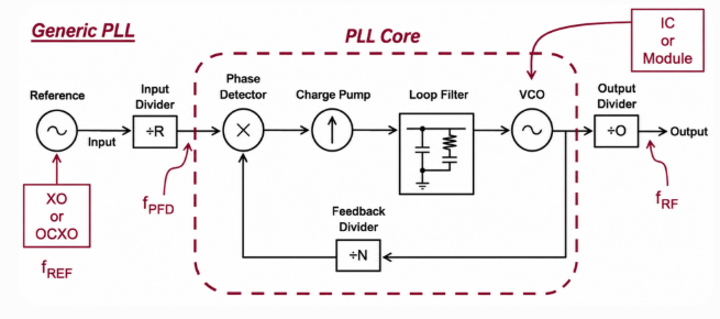
Figure 4. Relationship between a Crystal Oscillator Reference Clock and a PLL Synthesizer Timing System
One common misconception in clock system design is that PLL synthesizers completely replace crystal oscillators. In reality, most PLL-based timing systems still depend on a crystal oscillator as the stable reference clock source.
A crystal oscillator provides the low-noise reference clock that establishes baseline frequency stability for the entire timing architecture. The PLL synthesizer then multiplies, divides, or distributes that reference frequency to generate the system clocks required by processors, communication interfaces, and high-speed digital subsystems.
For example, a crystal oscillator may generate a stable 25 MHz reference clock, while the PLL synthesizer multiplies and distributes that signal to create synchronized outputs such as 100 MHz, 125 MHz, or other higher-frequency system clocks.
This combination allows electronic systems to achieve stable low-phase-noise timing while also supporting flexible multi-frequency clock generation across different digital subsystems.
Because PLLs rely on active feedback circuitry, the quality of the reference clock directly affects overall jitter and phase noise performance. A poorly designed reference clock path can degrade synchronization accuracy across the entire clock distribution network.
In many modern timing architectures, crystal oscillators and PLL synthesizers work together rather than compete directly. The crystal oscillator provides timing stability, while the PLL enables scalable clock management, synchronous clocking, and centralized clock distribution across complex digital systems.
Advantages of PLL Clock Synthesizers
Flexible Frequency Synthesis
PLL synthesizers can multiply or divide a reference clock to generate a wide range of output frequencies. This allows customized system timing for processors, communication interfaces, and digital subsystems operating at different speeds. Because the output frequency is programmable, PLL-based clock generator ICs are highly adaptable in systems where timing requirements may change during development or across different product variants.
Synchronized Clock Outputs
Many PLL synthesizers can generate multiple phase-aligned output clocks simultaneously. This is especially important in synchronous clocking systems where timing alignment between devices directly affects system stability and data integrity. Integrated clock distribution helps reduce clock skew, improve synchronization, simplify clock tree routing, and support complex multi-device timing architectures. These capabilities are commonly required in FPGA platforms, networking equipment, and high-speed digital systems.
Dynamic Frequency Scaling
PLL synthesizers support dynamic clock adjustment during system operation, allowing processors and digital systems to increase or reduce clock frequency depending on workload demands. Modern digital platforms rarely operate under constant workloads, especially in mobile processors, embedded computing systems, and power-sensitive electronics where performance, thermal output, and power consumption must be balanced continuously. Dynamic frequency scaling helps improve system efficiency while maintaining stable timing performance.
Improved System Integration
Modern PLL timing ICs often combine several clock management functions into a single device, including frequency synthesis, clock distribution, phase alignment, jitter attenuation, and spread-spectrum clocking. Integrating these timing functions into one centralized device helps reduce PCB complexity, simplify routing, and improve overall timing architecture scalability in high-speed electronic systems.
Reduced External Components
Instead of relying on multiple standalone oscillators, a single low-noise reference clock can be used together with a PLL synthesizer to generate several synchronized system clocks. This approach helps reduce PCB area, component count, routing complexity, and manufacturing cost. In compact or high-density electronic systems, minimizing the number of timing components can significantly simplify board-level design and improve overall integration efficiency.
Crystal Oscillator vs PLL Synthesizer: Detailed Performance Comparison
|
Parameter |
Crystal Oscillator (XO) |
PLL Synthesizer |
|
Frequency
Type |
Fixed
frequency |
Programmable
frequency |
|
RMS Jitter |
Typically
very low, often below 1 ps |
Higher
additive jitter depending on PLL design |
|
Phase Noise |
Lower phase
noise and cleaner spectral performance |
Depends on
VCO quality, loop bandwidth, and power integrity |
|
Frequency
Stability |
Excellent
long-term stability |
Depends
heavily on reference clock quality |
|
Clock Outputs |
Usually
single output |
Multiple
synchronized outputs |
|
Frequency
Scaling |
Not supported |
Supports
frequency multiplication and division |
|
Synchronization
Capability |
Limited in
multi-clock systems |
Strong
multi-device timing coordination |
|
Clock
Distribution |
Often
requires external timing ICs or buffers |
Frequently
integrated into the PLL device |
|
PCB
Complexity |
Simpler
routing and layout |
More advanced
timing architecture required |
|
Power
Consumption |
Lower |
Higher due to
active circuitry |
|
Noise
Sensitivity |
Less
sensitive to supply noise |
More
sensitive to power integrity and PCB noise |
|
Scalability |
Better for
simple systems |
Better for
complex digital platforms |
|
Typical
Applications |
RF systems,
ADC/DAC clocking, audio equipment, embedded electronics |
FPGA systems,
telecom infrastructure, Ethernet switches, SERDES platforms, high-speed
networking |
|
Main
Advantage |
Cleaner
low-noise timing |
Flexible
clock management and synchronization |
|
Main
Limitation |
Limited
frequency flexibility |
Higher jitter
and more complex implementation |
Engineering Tradeoffs Between PLLs and Crystal Oscillators
Figure 5. Phase Noise Comparison between XO, VCO, and PLL Output Signals
Choosing between a crystal oscillator and a PLL synthesizer is not simply a matter of selecting the “better” clock source. Each technology introduces different electrical tradeoffs that affect timing stability, PCB complexity, synchronization behavior, power sensitivity, and overall system performance. Understanding these differences is especially important in RF platforms, high-speed communication hardware, precision instrumentation, and modern digital timing architectures where clock behavior directly affects reliability and signal quality.
Jitter and Phase Noise Tradeoffs
Crystal oscillators usually produce lower intrinsic RMS jitter and cleaner phase noise because their signal path is relatively simple and does not rely on active feedback correction. This allows them to generate highly stable reference clocks with reduced short-term timing variation.
PLL synthesizers operate differently. They depend on voltage-controlled oscillators (VCOs), loop filters, divider networks, charge pumps, and feedback circuitry to generate controlled output frequencies. Because the PLL continuously adjusts its output to maintain phase alignment, additional timing noise can be introduced into the signal path.
In practical systems, this difference can directly affect timing behavior. Excessive jitter can reduce sampling precision in ADC systems, while increased phase noise can lower spectral clarity and degrade RF performance. PLL-based timing architectures may simplify overall synchronization, but poor loop design, excessive loop bandwidth, or inadequate power filtering can increase timing instability and waveform degradation.
Clock Distribution vs Signal Purity
Crystal oscillators provide excellent raw clock purity and are often used as stable low-noise reference sources. However, distributing timing signals across large systems using standalone oscillators can become increasingly difficult as routing complexity grows.
Multiple clock sources may require additional fanout buffers, clock dividers, and external timing ICs to maintain proper coordination between subsystems. As more devices are added, timing skew and routing complexity can become harder to control across the PCB.
PLL synthesizers simplify this process by supporting centralized timing management from a single reference source. Instead of relying on multiple independent oscillators, a PLL-based timing architecture can generate coordinated clocks for different subsystems while improving timing alignment across the design.
Even so, timing quality still depends heavily on PCB implementation. Long clock traces, noisy routing environments, weak grounding, and signal coupling can reduce timing stability regardless of the clock source itself.
Power Supply Sensitivity
Power integrity has a major impact on PLL performance. Noise on the supply rail can couple into the VCO and increase phase jitter, especially in high-frequency systems operating with tight timing margins.
Compared to crystal oscillators, PLL synthesizers are generally more sensitive to:
• switching regulator noise
• supply ripple
• ground bounce
• PCB coupling noise
Because of this, PLL-based systems often require cleaner analog supply rails, controlled PCB layout, local decoupling capacitors, and stronger power isolation techniques to maintain stable timing behavior.
Crystal oscillators are typically less sensitive to supply noise because their oscillation mechanism is more electrically isolated and less dependent on active correction circuitry.
Scalability and System ComplexityCrystal oscillators are ideal for simple fixed-frequency systems where only one or a few stable clocks are required. They offer straightforward implementation, simpler routing, and lower overall power consumption.
However, as timing architectures become more advanced, relying on several standalone oscillators can increase PCB congestion, BOM cost, routing difficulty, and timing coordination challenges.
PLL synthesizers scale more efficiently in systems that require coordinated timing across several operating frequencies. By generating multiple clocks from a common reference source, PLL-based architectures simplify timing management while reducing the number of external timing components needed throughout the design.
Frequency Accuracy and Stability
Frequency accuracy measures how closely a clock signal matches its intended operating frequency. It is commonly expressed in Parts Per Million (PPM), which describes how much the actual clock frequency can vary from its nominal value. Even small frequency deviations can affect synchronization reliability, sampling precision, data transfer stability, and long-term timing consistency in digital systems.
Crystal oscillators are widely used because they provide stable long-term frequency accuracy compared to many other clock generation methods. Their quartz resonator structure naturally maintains a consistent oscillation frequency, helping reduce timing drift caused by temperature variation, supply voltage fluctuation, crystal aging, and environmental conditions.
PLL synthesizers do not generate independent frequency accuracy on their own. Instead, they inherit the stability and accuracy of the reference crystal oscillator. When a PLL multiplies or divides the reference frequency, the relative PPM accuracy generally remains consistent even though the operating frequency changes.
This allows PLL systems to generate higher-frequency clock signals while maintaining the frequency stability of the original crystal reference source across the timing architecture.
However, frequency accuracy and signal purity are not identical. A PLL can preserve overall frequency accuracy while still introducing additional phase noise or additive jitter because of VCO behavior, loop bandwidth characteristics, feedback loop dynamics, and power supply sensitivity. As a result, a PLL output may maintain accurate average frequency stability while still exhibiting more short-term timing variation than the original crystal oscillator.
In practical electronic systems, poor frequency stability can create synchronization errors, timing drift, communication instability, and degraded overall system performance across multiple digital subsystems.
Which Clock Source Delivers Better Signal Integrity?
Signal integrity depends on more than whether a design uses a crystal oscillator or a PLL synthesizer. It also depends on jitter tolerance, phase noise requirements, power supply cleanliness, PCB routing quality, clock skew, and how many devices must share the same timing reference. In simple terms, a crystal oscillator usually provides the cleaner clock signal at the source, while a PLL synthesizer provides better timing coordination across complex digital systems.
Crystal Oscillators and Signal Purity- Crystal oscillators are usually the better choice when raw clock quality matters most. Because an XO generates a stable fixed-frequency clock using a simpler signal path, it typically provides cleaner timing characteristics and improved spectral stability compared to PLL-based clock sources. This is especially important in systems where clock behavior directly affects analog or RF performance.
In RF receivers, lower phase noise can improve receiver sensitivity and spectral clarity. In ADC systems, reduced timing variation can improve sampling accuracy and help preserve measurement resolution. In audio systems, cleaner timing can reduce distortion and unwanted noise artifacts. Because of these characteristics, crystal oscillators are often preferred in RF communication systems, precision ADC/DAC clocking, audio equipment, medical electronics, and measurement instruments where stable low-noise timing is more important than programmable frequency flexibility.
PLL Synthesizers and System- Level Timing Control- PLL synthesizers usually introduce more additive jitter than standalone crystal oscillators because they rely on active feedback circuitry, divider networks, and voltage-controlled oscillators. However, they provide much better system-level timing coordination in designs that require several operating frequencies across multiple devices.
In high-speed networking platforms, Ethernet switches, telecom equipment, and multi-board systems, the biggest timing challenge is often not simply generating the cleanest single clock signal. It is maintaining alignment across the entire timing architecture. A PLL synthesizer helps maintain coordinated timing relationships between clock domains while reducing synchronization errors and clock skew across devices.
For example, high-speed digital systems may require separate clocks for logic, memory, SERDES interfaces, and communication subsystems operating at different frequencies. In these situations, PLL-based timing ICs can simplify timing management more effectively than multiple independent crystal oscillators.
Practical Signal Integrity Tradeoff- The best clock source depends on the type of timing stability challenge the design is trying to solve. If the system is highly sensitive to noise, such as RF receivers, ADC sampling circuits, or professional audio equipment, a crystal oscillator is usually the stronger choice because it provides cleaner waveform behavior and lower timing variation.
If the design requires synchronization across several devices or multiple clock domains, a PLL synthesizer is often the better solution because it supports scalable timing coordination and centralized clock management across the system.
PCB Design Still Matters- Even a high-quality clock source can perform poorly if the PCB layout is not carefully designed. Long clock traces, poor grounding, inadequate decoupling, crosstalk from high-speed signals, and noisy power rails can all degrade timing stability and signal quality.
For crystal oscillators, poor routing can introduce noise into an otherwise clean reference clock. For PLL synthesizers, noisy supplies or weak decoupling can increase VCO noise, phase jitter, and timing instability across the timing network. Careful PCB routing, clean power delivery, proper grounding, and controlled impedance are important for maintaining stable system timing regardless of whether the design uses a crystal oscillator or a PLL synthesizer.
Common Problems in Clock System Design
Figure 6. Clock Skew and Synchronization Problems caused by Poor Timing Alignment in PCB Designs
1. Clock Skew
Clock skew occurs when the same clock signal arrives at different devices at slightly different times. In synchronous digital systems, excessive clock skew can create timing mismatches that lead to unstable operation or data corruption. Clock skew becomes more difficult to manage in multi-board systems, high-speed networking equipment, PCIe platforms, and large timing architectures. Poor clock tree design, unequal trace lengths, and excessive routing delays can all increase synchronization problems between devices.
2. EMI and Electromagnetic Interference
High-speed clock signals can generate electromagnetic interference (EMI) that affects nearby circuits and communication paths. Poorly controlled clock routing may introduce signal distortion, noise coupling, unstable RF performance, and increased radiated emissions.
PLL-based timing systems can be especially sensitive because high-frequency clock edges and switching activity may inject additional noise into the PCB environment. Careful grounding, impedance control, and spread-spectrum clocking techniques are often used to reduce EMI problems in dense electronic systems.
3. Crosstalk Between High-Speed Signals
Crosstalk occurs when high-speed clock traces interfere with nearby signal lines through capacitive or inductive coupling. In tightly packed PCB layouts, this can lead to increased jitter, timing instability, signal corruption, and reduced communication reliability.
Distributed timing systems operating at high frequencies are often vulnerable when routing distances are long or signal isolation is inadequate. Proper PCB spacing, controlled impedance routing, and dedicated ground references help minimize crosstalk issues.
4. Power Supply Noise
Clock performance depends heavily on power integrity. Noise from switching regulators, digital subsystems, or poorly filtered power rails can directly affect PLL stability and timing accuracy.
In PLL-based timing architectures, power supply noise can increase phase jitter, destabilize the VCO, reduce synchronization accuracy, and degrade overall timing consistency.
A noisy power rail can affect the entire timing network, especially in telecom, PCIe, and high-speed networking systems. To reduce these issues, low-noise regulators, local decoupling capacitors, power isolation techniques, and clean analog supply rails are commonly used.
5. PCB Layout Problems
Even high-quality clock generator ICs can perform poorly if the PCB layout is not optimized for signal integrity. Common layout mistakes include long clock traces, poor grounding, excessive vias, improper impedance control, and routing clocks near noisy digital signals.
In RF and precision timing systems, poor PCB layout can increase phase noise, worsen jitter performance, and reduce overall timing stability. Maintaining short clock paths and minimizing noise coupling are important for preserving clean synchronous clocking throughout the system.
6. Timing Violations
Timing violations occur when signals fail to meet setup or hold time requirements within digital systems. These problems are common in FPGA timing closure, high-speed memory interfaces, PCIe systems, and SERDES communication links.
Excessive jitter, clock skew, or unstable clock distribution can all contribute to timing failures.
In complex digital platforms, even small clock integrity problems can propagate throughout the timing architecture and create intermittent system instability that is difficult to diagnose. Because of this, careful clock management and signal integrity analysis are important in modern high-speed electronic design.
Common Applications of PLL Synthesizers and XO Clocks
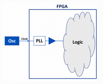
Figure 7. Basic FPGA Timing Architecture using an Oscillator and PLL
Different clock generation technologies are optimized for different timing requirements. The best solution depends on factors such as signal integrity, synchronization complexity, frequency flexibility, and overall system timing architecture.
|
Application |
Preferred
Clock Solution |
Main
Reason |
|
Embedded Microcontrollers |
Crystal Oscillator |
Simple low-power fixed-frequency
timing |
|
RF Receivers |
Crystal Oscillator |
Lower phase noise and improved
receiver sensitivity |
|
Precision ADC/DAC Systems |
Crystal Oscillator |
Lower RMS jitter for accurate
sampling |
|
Audio Processing Equipment |
Crystal Oscillator |
Cleaner waveform stability and
lower distortion |
|
FPGA Platforms |
PLL Synthesizer |
Multiple synchronized clock
domains |
|
Ethernet Switches |
PLL Synthesizer |
Centralized clock distribution |
|
Telecom Infrastructure |
PLL Synthesizer |
High fanout synchronous timing |
|
Data Center Networking |
PLL Synthesizer |
Scalable timing architecture |
|
Multi-Board Systems |
PLL Synthesizer |
Improved synchronization across
devices |
|
Everyday
Electronics |
Crystal Oscillator |
Lower cost and simplified PCB
design |
Example: FPGA Timing Architecture Using a PLL Synthesizer
A practical example of PLL-based clock management can be seen in high-speed FPGA systems. Modern FPGA platforms often require several operating frequencies for different subsystems running at the same time.
For example, a single FPGA board may require:
• 100 MHz for internal logic processing
• 125 MHz for Ethernet communication
• 156.25 MHz for SERDES interfaces
Additional clocks for memory controllers and peripheral interfaces
Using separate crystal oscillators for each frequency can increase PCB congestion, routing complexity, power consumption, and clock skew between timing domains. As the number of independent clock sources increases, maintaining stable synchronization across the system also becomes more difficult.
Instead, many FPGA timing architectures use a low-noise 25 MHz crystal oscillator together with a PLL synthesizer. The crystal oscillator provides the stable reference clock, while the PLL synthesizer multiplies and distributes that signal into multiple coordinated output frequencies across the FPGA platform.
This approach simplifies clock tree routing, reduces the number of external timing components, improves synchronization accuracy, and helps maintain more consistent timing relationships between subsystems.
In high-speed digital systems, this type of centralized timing architecture is often easier to scale and manage than using several standalone crystal oscillators operating independently.
When to Use a Crystal Oscillator vs PLL Synthesizer
Choosing between a crystal oscillator and a PLL synthesizer depends on the complexity of the system, timing requirements, and the number of clock signals needed throughout the design.
A crystal oscillator is usually the better choice when a system only needs one stable clock frequency and does not require advanced timing management. Crystal oscillators are simpler to implement, consume less power, and provide cleaner fixed-frequency timing performance. Because of their stable waveform quality, they are commonly used in embedded systems, RF communication devices, ADC and DAC clocking, commercial electronics, and precision instrumentation where timing accuracy is important.
Crystal oscillators are ideal for designs that prioritize fixed-frequency operation, low timing variation, reduced phase noise, simple PCB layout, and lower power consumption.
In contrast, a PLL synthesizer is better suited for systems that require scalable timing coordination across several devices, programmable frequencies, or centralized clock routing throughout the design.
PLL-based timing architectures are commonly used in Ethernet switches, telecom infrastructure, SERDES systems, and high-speed digital platforms where synchronization and scalable timing management are important.
For example, high-speed digital systems often require several phase-aligned clocks operating at different frequencies. Using multiple standalone crystal oscillators in these designs can increase routing complexity, clock skew, and PCB congestion.
A PLL clock generator IC can simplify the timing architecture by improving coordination between several operating frequencies from one stable reference source.
PLL synthesizers are typically preferred in systems that require multiple clock domains, frequency scaling, high fanout clock distribution, synchronous multi-device operation, and advanced clock management.
Although PLL synthesizers usually introduce more additive jitter than standalone crystal oscillators, their flexibility and scalability make them highly valuable in many modern electronic systems, especially where complex timing coordination is required.
Choosing the Right System Clock for Your Application
Selecting the right clock source depends heavily on overall system timing requirements, synchronization complexity, power constraints, and signal integrity goals. Important considerations include frequency requirements, jitter tolerance, the number of clock outputs, PCB space limitations, cost targets, and long-term system scalability.
A crystal oscillator is usually the better choice when low jitter is important, a single fixed frequency is sufficient, system simplicity is preferred, and power consumption must remain low. Crystal oscillators are often used in applications where clean signal quality and straightforward timing architecture are more valuable than programmable clock flexibility.
A PLL synthesizer is generally the better option when a system requires multiple synchronized clocks, programmable frequency scaling, complex clock distribution, or reduced PCB space through centralized timing management. PLL-based timing architectures are commonly used in high-speed digital systems where several devices or subsystems must remain synchronized across different operating frequencies.
Conclusion
Crystal oscillators and PLL synthesizers are both widely used for system timing, but each one is designed for different application needs. Crystal oscillators are usually preferred for stable fixed-frequency operation, lower jitter, cleaner timing signals, and simpler PCB design. PLL synthesizers provide greater flexibility for systems that require programmable frequencies, multiple clock domains, and advanced timing coordination across several devices. Understanding the differences between these clock solutions helps improve timing stability, signal quality, and overall system reliability.
test funkcji.Najwyższe opłacalne produkty i najlepsza usługa to nasze wieczne zaangażowanie.
Hot Artykuł
- LM358 Dualny wzmacniacz operacyjny Kompleksowy przewodnik: Pinouts, diagramy obwodów, odpowiedniki, przydatne przykłady
- Czy CR2032 i CR2016 są wymienne?
- Zrozumienie różnic ESP32 i Analiza techniczna i ESP32-S3
- Wybór odpowiedniej baterii: Przewodnik po AG4, LR626, LR66, 177/376/377, SR626 i SR626SW
- Podstawy tranzystorów BC547: układ pinów, obwody aplikacyjne, modele alternatywne/uzupełniające
- NPN vs. PNP: Jaka jest różnica?
- ESP32 vs STM32: Który mikrokontroler jest dla Ciebie lepszy?
- Co to jest MOSFET i jak to działa?
- Przekaźnik elektryczny Podstawowy: Działanie, typy i zastosowania
- Tranzystory PNP: struktura, zasada pracy i zastosowanie
 Solid State Relay vs Mechanical Relay: Key Differences, Uses, and How to Choose
2026-05-07
 Zrozumienie PLA do druku 3D
2026-05-06
Często Zadawane Pytania [FAQ]
1. Why are crystal oscillators preferred in RF and ADC applications?
Crystal oscillators are preferred because they usually produce lower jitter and reduced phase noise. In RF receivers, this improves receiver sensitivity and signal clarity, while in ADC systems it helps improve sampling accuracy and measurement performance.
2. How does clock jitter affect system performance?
Clock jitter creates short-term timing variation in clock signals. Excessive jitter can reduce communication reliability, increase timing errors, lower ADC accuracy, and create synchronization problems in high-speed digital systems.
3. Why is PCB layout important in clock system design?
Even a high-quality clock source can perform poorly if the PCB layout is not optimized. Long traces, noisy power rails, poor grounding, and weak decoupling can increase jitter, phase noise, EMI, and timing instability.
4. How do PLL synthesizers help reduce system complexity?
A PLL synthesizer can generate several coordinated clock frequencies from one reference clock source. This reduces the number of external oscillators, simplifies clock routing, lowers PCB congestion, and improves timing scalability.
5. Why is power supply noise a problem for PLL systems?
PLL synthesizers are sensitive to power supply noise because voltage fluctuations can affect the VCO and feedback circuitry. This may increase phase jitter, reduce synchronization accuracy, and destabilize the timing network.
6. Why do modern electronic systems often combine PLLs and crystal oscillators?
Many systems combine both technologies because they serve different purposes. The crystal oscillator provides stable reference timing, while the PLL synthesizer manages frequency generation, synchronization, and clock distribution across the system.
Gorący numer części
 C1608X7S0J475K080AC
 GCJ188R72A332KA01D
 GRM0225C1E6R9WA03L
 C1005C0G2A121K050BA
 CGA9N4X7R2J224K230KE
 GRM32EC81C476ME15L
 GRM0335C1H5R2BA01D
 08053A680JAT2A
- 08053C271JAT2A
 GRM1555C1H330FA01J
- 12105U221JAT2A
- TAP156M020CCS
- SMAJ33A
- 9DBL0651BKILF
- MT9044AP1
- MT29F64G08CBABBWP-12:B
- ATF1500A-10JC
- EPM7512BQC208-5
- TLD5045EJXUMA1
- MAX749CSA
- RT0805BRE07270RL
- 6MBI150J-120
- N282CH24
- VI-JN1-EY/F2
- AD7720BRUZ
- ADS5203IPFBR
- TPS7A6333QDRKRQ1
- MAX3232CDWR
- AD8541ARZ
- BB664-02VE7902
- ICS950952BGLFT
- ISPLSI2064E-100LTN100
- MC100EP210SFA
- NH82801GBM/SL8YB
- S34ML01G200TF100
- S5H1420X01-E0RZ
- SAF-C164CI-LM CA+
- SB5504ML
- SN761680DBTRG4
- TC74AC175F
- ZPSD301-B-90LI
- CSC0105A-01S28
- ET16312N
- M15F1G1664A-8CB
- TC9412AF
- TNETX3151PGV
- NAND98R3M0BZBB5E
- S87C752-1A28
- HG-0814